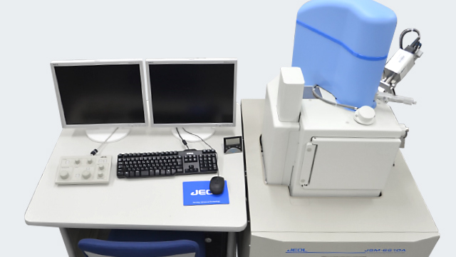
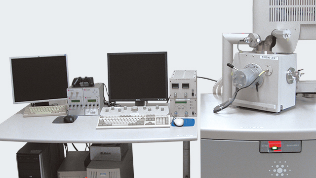
Reaction science high-voltage scanning transmission electron microscope JEM 1000K RS
A reaction science high-voltage scanning transmission electron microscope can penetrate very thick samples compared to a typical 200-kV electron microscope. In particular, a major feature of this device is that it allows in situ observations of chemical reactions such as metal oxidation and catalytic reactions by various gases.
Read more
|
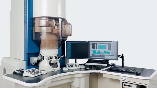
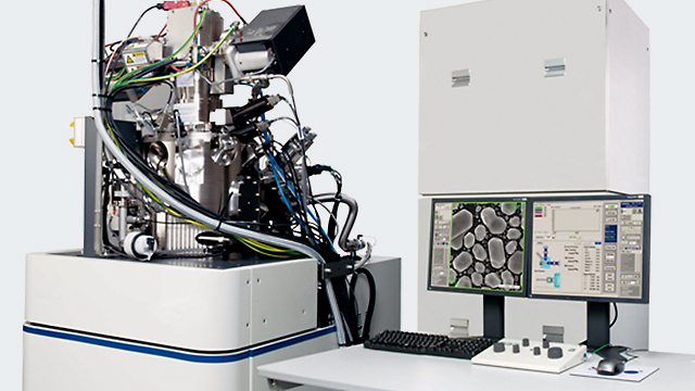
High-resolution analytical scanning transmission electron microscope JEM-ARM200 (Cold) (aberration correcting electron microscope)
An atomic resolution analysis electron microscope with the world's highest STEM-HAADF image resolution of 78 pm is equipped with a spherical aberration corrector in the irradiation system. When used together with EDS or EELS, atomic-level elemental analysis is possible.
|
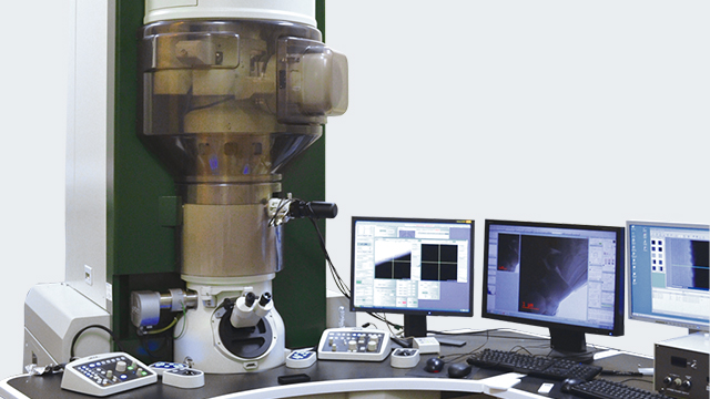
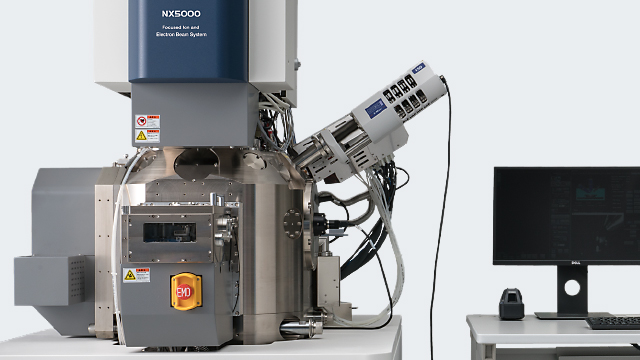
Field emission scanning transmission electron microscope JEM-10000BU (aberration correcting electron microscope)
An atomic resolution analysis electron microscope with the world's highest TEM/STEM image resolution is equipped with a spherical aberration corrector in the irradiation system and objective system. When used together with EDS or EELS, atomic-level elemental analysis is possible.
Read more
|
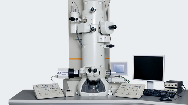
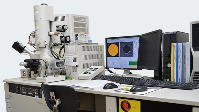
Electron spectroscopy scanning transmission electron microscope EM2100M
An electron microscope with an accelerating voltage of 200 kV can be attached to a wavelength dispersive X-ray spectrometer (WDX) in addition to EELS. It can measure cathodoluminescence (CL) light.
Read more
|
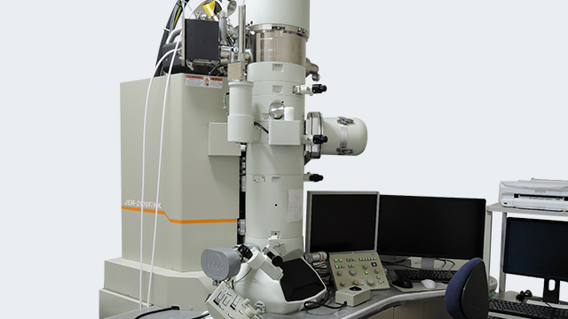
Field emission transmission electron microscope JEM-2100F/HK
A field emission electron microscope with an acceleration voltage of 200 kV has a high resolution. It can provide observations with up to 1.5 million times direct magnification when using the TEM function.
Read more
|
Scanning electron microscope Quanta200FEG
A scanning electron microscope enables SEM observations while controlling the atmosphere, except for a vacuum. EDS provides elemental analysis and sample manipulation functions.
|